請先看『使用說明』
IO Device:F75111 CIO Utility Console under linux
From LEXWiKi
(→The Sample code source you can download from) |
(→The Sample code source you can download from) |
||
| (20 intermediate revisions not shown.) | |||
| Line 2: | Line 2: | ||
== The Sample code source you can download from == | == The Sample code source you can download from == | ||
| - | + | <!-- | |
<Google Drive> | <Google Drive> | ||
| - | Source file: [https://drive.google.com/file/d/ | + | Source file: [https://drive.google.com/file/d/14QO67ToUVpBndn1U3ViwP1s8UgnSTnI2/view?usp=sharing CIO_Utility_Console_v1.7.0_Src] |
| - | Binary file: [https://drive.google.com/file/d/ | + | Binary file: [https://drive.google.com/file/d/1OGTsRTM-uyTJUyxBrvw0_AASck2Sgu-t/view?usp=sharing CIO_Utility_Console_v1.7.0_Bin] |
| + | --> | ||
<FTP> | <FTP> | ||
| - | Source file: [ftp://ftp.lex.com.tw/Engineer/SoftSupport/AP_Module/CIO_Uitlity/linux_base/console/CIO_Utility_Console_L_Src_v1. | + | Source file: [ftp://ftp.lex.com.tw/Engineer/SoftSupport/AP_Module/CIO_Uitlity/linux_base/console/CIO_Utility_Console_L_Src_v1.7.0.zip CIO_Utility_Console_v1.7.0_Src] |
| - | Binary file: [ftp://ftp.lex.com.tw/Engineer/SoftSupport/AP_Module/CIO_Uitlity/linux_base/console/CIO_Utility_Console_L_Bin_v1. | + | Binary file: [ftp://ftp.lex.com.tw/Engineer/SoftSupport/AP_Module/CIO_Uitlity/linux_base/console/CIO_Utility_Console_L_Bin_v1.7.0.zip CIO_Utility_Console_v1.7.0_Bin] |
== MB Support List == | == MB Support List == | ||
| Line 145: | Line 146: | ||
== How to use this Demo Application == | == How to use this Demo Application == | ||
| - | [[Image:CIO Utility console | + | [[Image:CIO Utility console.jpg]]<br/> |
[[Image:CIO208.jpg]]<br/> | [[Image:CIO208.jpg]]<br/> | ||
| - | + | === Step1. Unzip "CIO_Utility_Console_L_Bin_v1.7.0.zip" and change user permission === | |
| - | + | The program must control I/O device. You must change user permission to "'''root'''". You could use this command "'''sudo su'''"<br/> | |
| + | |||
| + | === Step2. Execute program === | ||
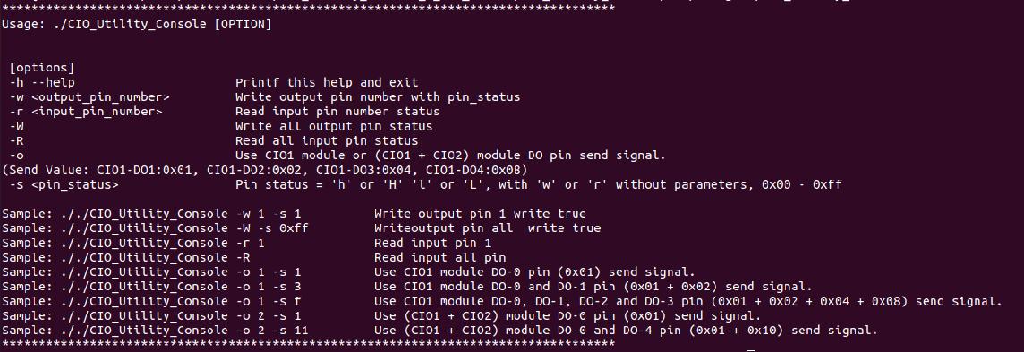
| + | Enter "'''./CIO_Utility_console -h'''" to show help menu.<br/> | ||
Example:<br/> | Example:<br/> | ||
| - | CIO_Utility_console -- | + | CIO_Utility_console -w 1 -s h<br/> |
| + | CIO_Utility_console -r 1<br/> | ||
| + | CIO_Utility_console -W -s 0x0f<br/> | ||
| + | CIO_Utility_console -R<br/> | ||
| + | |||
| + | === Step3. Use'-o' to simple set F75111 DO pin status to high or low === | ||
| + | Enter "'''./CIO_Utility_console -o <CIO_SN> -s <Pin_Status>'''" to set DO pin status.<br/> | ||
| + | |||
| + | <br/> | ||
| + | Pin_Status use 1 byte to indicate the status of the Pin.<br/> | ||
| + | DO-0 is bit0, DO-1 is bit1, DO-2 is bit2 and DO-3 is bit3.<br/> | ||
| + | |||
| + | If Pin_Status value is 0x01 (0000 0001), means DO-0 pin will be set to high. Other pins will be set to low.<br/> | ||
| + | Example: "'''./CIO_Utility_console -o 1 -s 1'''" means set CIO1 module DO-0 pin (0x01) status to high. And other pins to low.<br/> | ||
| + | |||
| + | If Pin_Status value is 0x03 (0000 0011), means DO-0 and DO-1 pin will be set to high. Other pins will be set to low.<br/> | ||
| + | Example: "'''./CIO_Utility_console -o 1 -s 3'''" means set CIO1 module DO-0 and DO-1 pin (0x01 + 0x02) status to high. And other pins to low.<br/> | ||
| + | |||
| + | If Pin_Status value is 0x0f (0000 1111), means DO-0, DO-1, DO-2, DO-3 pins will be set to high. No pin will be set to low.<br/> | ||
| + | Example: "'''./CIO_Utility_console -o 1 -s f'''" means set CIO1 module DO-0, DO-1, DO-2 and DO-3 pin (0x01 + 0x02 + 0x04 + 0x08) status will be set to high. No pin set to low.<br/> | ||
| + | |||
| + | If Pin_Status value is 0x00 (0000 0000), means DO-0, DO-1, DO-2, DO-3 pins will be set to low. No pin will be set to high.<br/> | ||
| + | Example: "'''./CIO_Utility_console -o 1 -s 0'''" means set CIO1 module DO-0, DO-1, DO-2 and DO-3 pin status will be set to low. No pin set to high.<br/> | ||
== F75111 Layout Picture == | == F75111 Layout Picture == | ||
| Line 161: | Line 187: | ||
and Enable WDT function pin | and Enable WDT function pin | ||
| - | === | + | === Base on libF75111.a API function as below list === |
| - | + | bool F75111_Init(); | |
| - | + | bool F75111_4I4O_Init(); | |
| - | + | bool F75111_8I8O_Init(); | |
| - | + | ||
| - | + | bool F75111_GetDigitalInput_Pin(int); //pin number 0-15 | |
| - | + | BYTE F75111_GetDigitalInput(); | |
| - | + | BYTE F75111_GetDigitalInput_4I4O(); //4I4O(CIO1) | |
| - | + | BYTE F75111_GetDigitalInput_8I8O(); //8I(CIO1)+8O(CIO2) | |
| - | + | ||
| - | + | bool F75111_SetDigitalOutput_Pin(BYTE pin_number,bool pin_status); | |
| - | + | void F75111_SetDigitalOutput(BYTE byteValue); | |
| - | + | void F75111_SetDigitalOutput_4I4O(BYTE byteValue);//20190828 add by Nico ,20200430 kk update | |
| - | + | void F75111_SetDigitalOutput_8I8O(BYTE byteValue); | |
| - | + | void F75111_SetDigitalOutput_1i1o(BYTE byteValue);//20200504 jimmy update for wet3901 | |
| - | + | ||
| - | + | BYTE F75111_GetWDTMode(); | |
| - | + | void F75111_SetWDTMode(BYTE dwvalue); | |
| - | + | ||
| - | + | void F75111_SetWDTEnable (BYTE byteTimer); | |
| - | + | void F75111_SetWDTDisable (); | |
| - | + | ||
| - | + | ||
| - | + | ||
| - | + | ||
| - | + | ||
| - | + | ||
| - | + | ||
| - | + | ||
| - | + | ||
| - | + | ||
| - | void | + | |
| - | + | ||
| - | + | ||
| - | + | ||
| - | + | ||
| - | + | ||
| - | + | ||
| - | + | ||
| - | + | ||
| - | + | ||
| - | + | ||
| - | + | ||
| - | + | ||
| - | + | ||
| - | + | ||
| - | + | ||
| - | + | ||
| - | + | ||
| - | + | ||
| - | + | ||
| - | + | ||
| - | + | ||
| - | + | ||
| - | + | ||
| - | + | ||
| - | + | ||
| - | + | ||
| - | + | ||
| - | + | ||
| - | + | ||
| - | + | ||
| - | + | ||
| - | + | ||
| - | + | ||
| - | + | ||
| - | + | ||
| - | + | ||
| - | + | ||
| - | + | ||
| - | + | ||
| - | + | ||
| - | + | ||
| - | + | ||
| - | + | ||
| - | + | ||
| - | + | ||
| - | + | ||
| - | + | ||
| - | + | ||
| - | + | ||
| - | + | ||
| - | + | ||
| - | + | ||
| - | + | ||
| - | + | ||
| - | + | ||
| - | + | ||
| - | + | ||
| - | + | ||
| - | + | ||
| - | + | ||
| - | + | ||
| - | + | ||
| - | + | ||
| - | + | ||
| - | + | ||
| - | + | ||
| - | + | ||
| - | + | ||
| - | + | ||
| - | + | ||
| - | + | ||
| - | + | ||
| - | + | ||
| - | + | ||
| - | + | ||
| - | + | ||
| - | + | ||
| - | + | ||
| - | + | ||
| - | + | ||
| - | + | ||
| - | + | ||
| - | + | ||
| - | + | ||
| - | + | ||
| - | + | ||
| - | + | ||
| - | + | ||
| - | + | ||
| - | + | ||
| - | + | ||
| - | + | ||
| - | + | ||
Current revision
Contents |
The Sample code source you can download from
<FTP>
Source file: CIO_Utility_Console_v1.7.0_Src
Binary file: CIO_Utility_Console_v1.7.0_Bin
MB Support List
| Ivybridge | BayTrail | Apollo Lake | Skylake/Kabylake | Card |
|---|---|---|---|---|
|
2I847H |
1I385A/H |
2I390CW |
2I610DW/HW |
CIO116-G |
|
3I8347A/CW |
1I386HW |
2I390CW |
2I610HW |
E691A |
|
3I847NX/NM |
2I380A/NX |
3I390AW |
3I610DW | |
|
3I847D(OEM) |
2I382A |
3I390D(OEM) |
PM610DW | |
|
3I847HW |
2I385A/BW/CW/EW/HW/PW |
3I390NX |
ST610W | |
|
CI847A/C |
3I380A/CW/D/NX |
3I393NX |
3I170DW/HW/NX | |
|
3I770A/CW |
3I385AW/CW |
PM390CW |
CI170A/C | |
|
CI770A/C |
ST385W |
PM170DW |
How to use this Demo Application
Step1. Unzip "CIO_Utility_Console_L_Bin_v1.7.0.zip" and change user permission
The program must control I/O device. You must change user permission to "root". You could use this command "sudo su"
Step2. Execute program
Enter "./CIO_Utility_console -h" to show help menu.
Example:
CIO_Utility_console -w 1 -s h
CIO_Utility_console -r 1
CIO_Utility_console -W -s 0x0f
CIO_Utility_console -R
Step3. Use'-o' to simple set F75111 DO pin status to high or low
Enter "./CIO_Utility_console -o <CIO_SN> -s <Pin_Status>" to set DO pin status.
Pin_Status use 1 byte to indicate the status of the Pin.
DO-0 is bit0, DO-1 is bit1, DO-2 is bit2 and DO-3 is bit3.
If Pin_Status value is 0x01 (0000 0001), means DO-0 pin will be set to high. Other pins will be set to low.
Example: "./CIO_Utility_console -o 1 -s 1" means set CIO1 module DO-0 pin (0x01) status to high. And other pins to low.
If Pin_Status value is 0x03 (0000 0011), means DO-0 and DO-1 pin will be set to high. Other pins will be set to low.
Example: "./CIO_Utility_console -o 1 -s 3" means set CIO1 module DO-0 and DO-1 pin (0x01 + 0x02) status to high. And other pins to low.
If Pin_Status value is 0x0f (0000 1111), means DO-0, DO-1, DO-2, DO-3 pins will be set to high. No pin will be set to low.
Example: "./CIO_Utility_console -o 1 -s f" means set CIO1 module DO-0, DO-1, DO-2 and DO-3 pin (0x01 + 0x02 + 0x04 + 0x08) status will be set to high. No pin set to low.
If Pin_Status value is 0x00 (0000 0000), means DO-0, DO-1, DO-2, DO-3 pins will be set to low. No pin will be set to high.
Example: "./CIO_Utility_console -o 1 -s 0" means set CIO1 module DO-0, DO-1, DO-2 and DO-3 pin status will be set to low. No pin set to high.
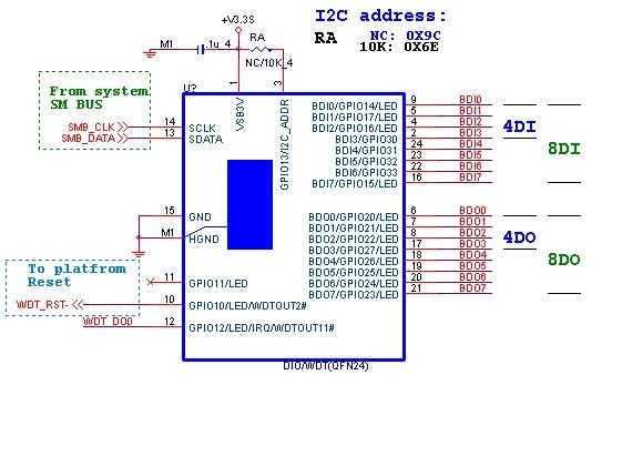
F75111 Layout Picture
Introduction
Initial Internal F75111 port address (0x9c)
   define GPIO1X, GPIO2X, GPIO3X to input or output
   and Enable WDT function pin
Base on libF75111.a API function as below list
bool	F75111_Init();
bool	F75111_4I4O_Init();
bool	F75111_8I8O_Init();

bool	F75111_GetDigitalInput_Pin(int);	//pin number 0-15
BYTE	F75111_GetDigitalInput();
BYTE	F75111_GetDigitalInput_4I4O();          //4I4O(CIO1)
BYTE	F75111_GetDigitalInput_8I8O();          //8I(CIO1)+8O(CIO2)

bool	F75111_SetDigitalOutput_Pin(BYTE pin_number,bool pin_status);
void	F75111_SetDigitalOutput(BYTE byteValue);
void    F75111_SetDigitalOutput_4I4O(BYTE byteValue);//20190828 add by Nico ,20200430 kk update
void	F75111_SetDigitalOutput_8I8O(BYTE byteValue);
void	F75111_SetDigitalOutput_1i1o(BYTE byteValue);//20200504 jimmy update for wet3901

BYTE	F75111_GetWDTMode();
void	F75111_SetWDTMode(BYTE dwvalue);

void	F75111_SetWDTEnable    (BYTE byteTimer);
void	F75111_SetWDTDisable   ();


